| Research Facilities | |
|---|---|
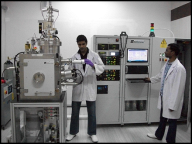 |
Dual Ion Beam Sputtering (DIBS) system: High crystalline-quality deposition of semiconductors and dielectrics |
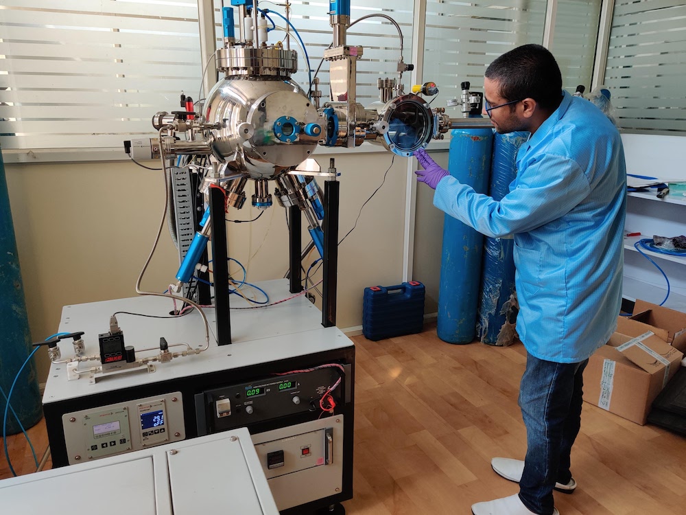 |
DC magnetron sputtering system: Desposition of metals for interconnects and electrode formation |
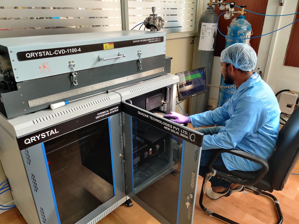 |
Chemical Vapor Deposition (CVD) system: High-quality deposition of two-dimensional (2D) transition metal dichalcogenides (TMDs) |
| |
Spin Coater: Thin-film deposition technique in which material is grown by sol-gel and hydrothermal method |
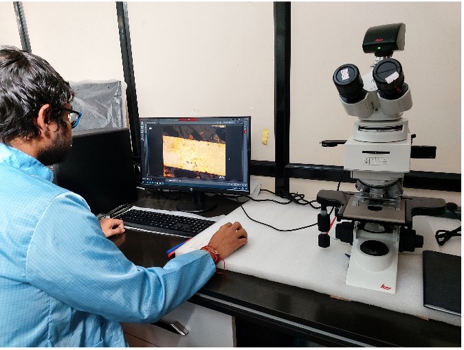 |
Digital Microscope: Precise 2D and 3D morphological analysis of microstructures |
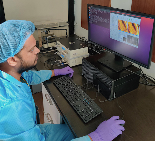 |
Scanning Tunneling Microscope (STM): Morphological inspection at the atomic scale |
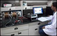 |
Four Probe Hall Measurement System: To measure: carrier concentration, type of doping, carrier mobility |
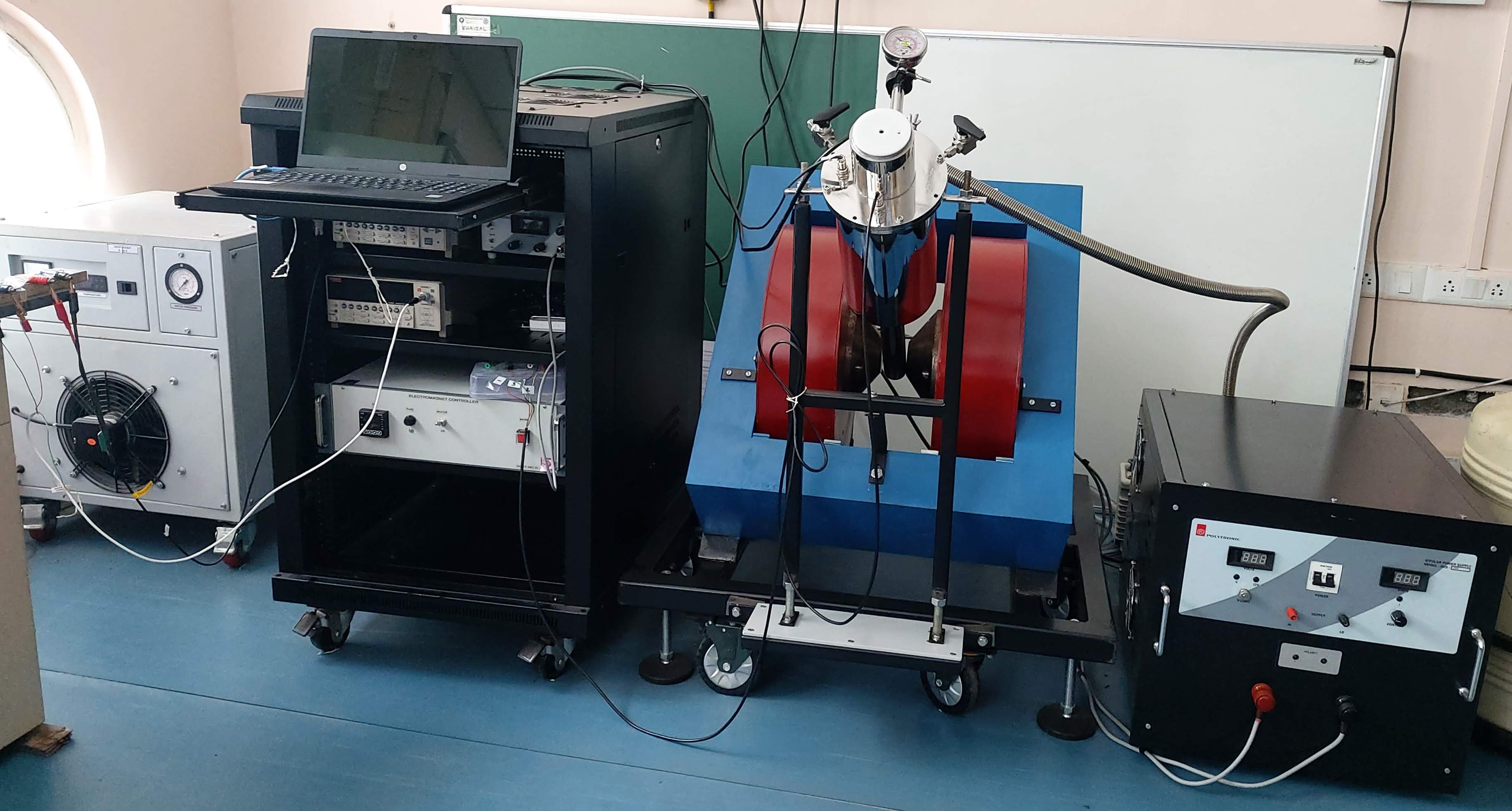 |
Carrier Transport Measurement at Varied Temperature: To measure: carried dynamics at different ambient temperature |
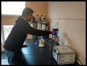 |
Gas and VOC Sensor Set-up: Resistive and capacitive sensitivity measurement set-up |
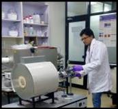 |
Rapid Thermal Processing (RTP): Rapid thermal annealing under various gas atmoshphere |
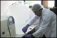 |
De-ionized Water: Remove particulates > 0.5 micron, ions, organics and bacteria Conductivity upto 1 uS/cm |
| |
Convection Oven: Temperature range: Upto 300 oC |
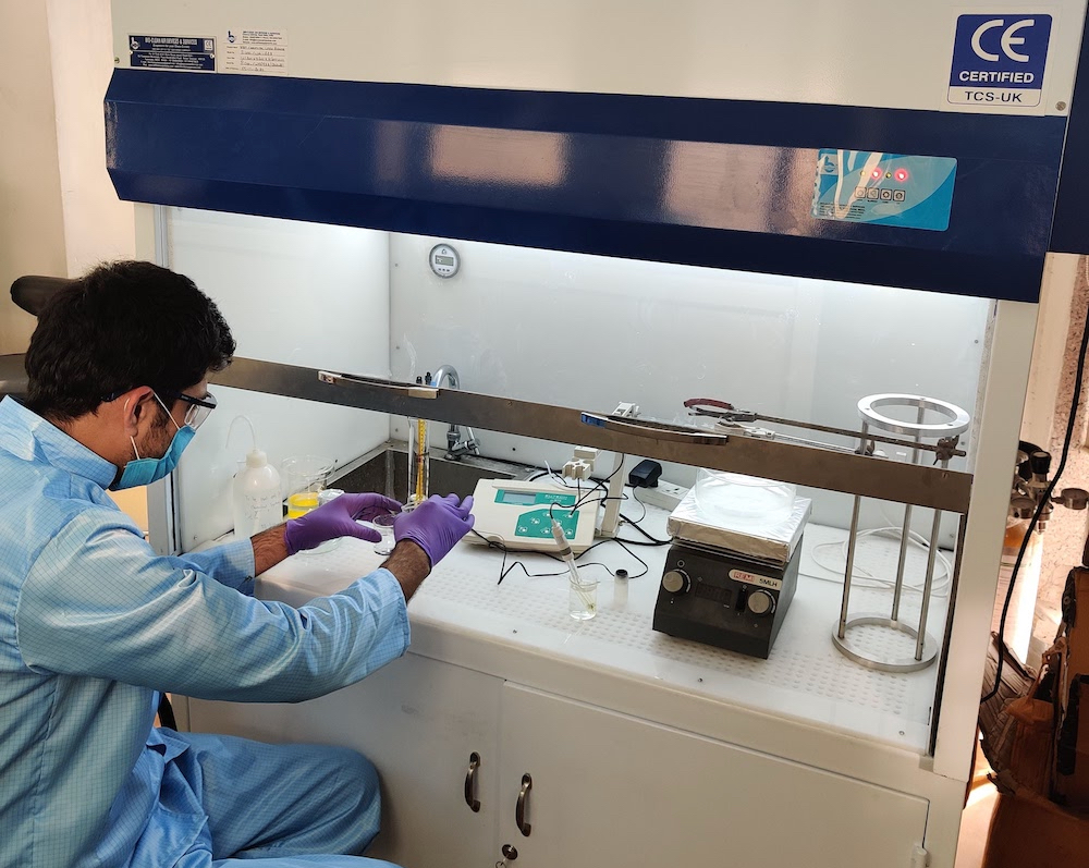 |
Fumehood with Blower: To perform: Wet chemical processing |
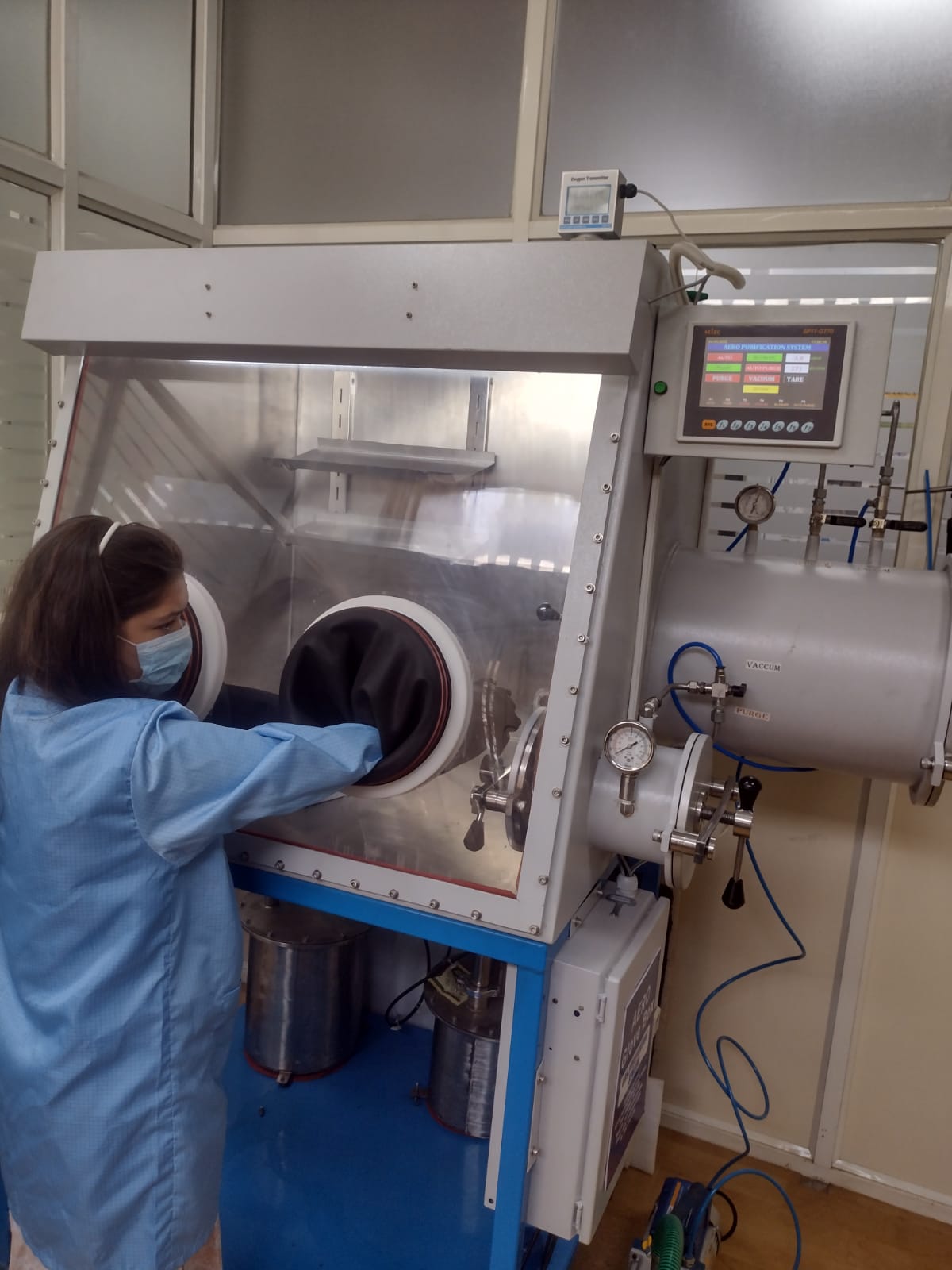 |
Glove box: To perform: Wet chemical processing and sample storage in Ar atmosphere |
| |
Keithley 4200A-SCS Parameter Analyzer: The Semiconductor parametric analyzer, delivers synchronizing current-voltage (I-V), capacitance-voltage (C-V) and ultra-fast pulsed I-V measurements |
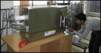 |
Annealing Furnace: To perform: Annealing (up to 1000 oC) under vacuum or gas atmosphere |
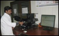 |
Variable-angle, Variable-wavelength Spectroscopic Ellipsometry: To measure: transmission, reflection, thickness, optical properties of materials |
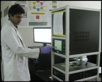 |
Solar Simulator System: To measure: VOC, ISC and PCE of solar cells at different temperature |
| |
Quantum Efficiency Measurement System: To measure: A monolithic, turnkey solution for photovoltaic material and device spectral characterization including EQE and IQE |
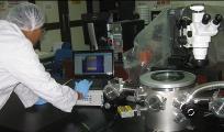 |
Cryogenic Vacuum Probe Station: To measure: Device characteristics at different ambient conditions |
| |
Computational Work Station: Device simulation such as Density Functional Theory, MOSFET, BJT, OFET, LED, Quantum well, Solar Cell, TFT, OTFT, OLED |
© 2010 Hybrid Nanodevice Research Group (HNRG) @ IIT Indore. All rights reserved.